MEMS Manufacturing Technology
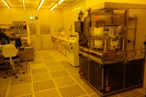
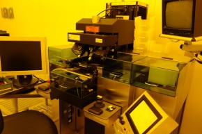
Protron Mikrotechnik works with all standard MEMS processes for silicon micromachining. Furthermore we use state of the art equipment for test and characterisation to offer processes and products with best possible quality.
Photolithography
- minimum structure width 1µm
Deposition and Thermal Processing
- Oxidation Diffusion, Annealing
- Low Pressure Chemical Vapor Deposition
- Plasma Enhanced Chemical Vapor Deposition
- Sputtering, Evaporation
- Electroplating
Etching
- Deep Reactive Ion Etching
- Reactive Ion Etching
- Wet Etching
- Ion Milling Etching
Wafer Bonding
- silicon fusion bonding
- anodic bonding
- eutectic bonding
Assembly and Packaging Technology
- waferdicing
- chipbonding
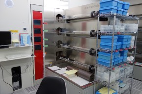
- wirebonding
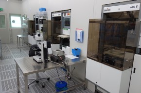
Test and Characterisation
- wafer prober
- 3D measurement system
- film-thickness measurement tools
- step height prober
- surface profiler
- film stress measurement system
- 4-point resistivity prober
- scanning electron microscope (SEM)
- pressure test chamber
- climatic exposure test cabinet